|
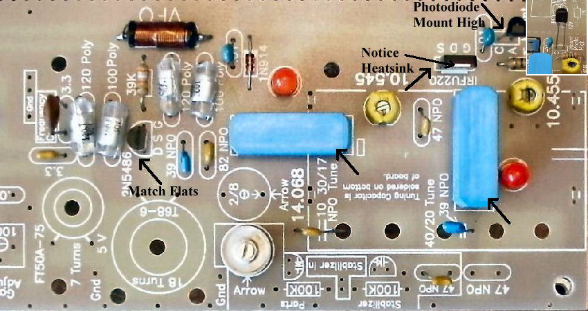
This is a Board 1 replacement for the Electroluminescent Receiver. It has provisions for mounting a PIC 16F628 DDS VFO based on a simplified PIC-EL DDS VFO, developed by VK5TM (the VK5TM simplified PIC-EL). The PIC EL project will work with the same PIC. It can also accept the output of any DDS VFO without the need of an amplifier after the DDS chip (AD9850 or AD9851). The board can be used with the Vackar VFO, same as the ELR receiver, or a DDS VFO. A slide switch at the First VFO Amplifier allows switching between the Vackar VFO and an external DDS VFO. 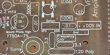 The BandPass Filters have been modified to cover 40 to 10 Meters. With the Vackar VFO, the receiver will cover the original 40, 30, 20, and 17 Meters and has the original IR connections to the Crystal Filters for switching the VFO frequency and the Crystal Oscillator frequency.  Using a DDS VFO allows coverage of all the bands covered with the new BandPass Filters - 40 through 10 Meters. Since they are varicap tuned, the coverage is continuous from 7MHz to 30MHz, allowing SWL reception. An AM detector or a regen detector can be added for listening to SWL stations. A transmitter function was added to the PIC-EL DDS VFO that removes the offset from the DDS frequency when a Key output is grounded. This activates a relay at the end of the VFO amplifiers that sends the DDS output to a Transmit Out connection which to sent to the input of your choice of amplifier and lowpass filters. The output is about 200 mV. See Transmitter to Interface with the SLR for connecting to a Novice tube type transmitter, QRP amplifiers and QRO amplifiers. This board uses one additional IR connection, between the First Mixer and the First VFO Amplifier, used as a feedback control to level the output of the VFO to about 4 Volts P-P across the entire 40 to 10 Meter bandwidth. The level is adjusted by a 500K trimmer at the First VFO Amplifier. See Adjusting the 500K pot at the MOSFET Amplifier with the IR link at the bottom of the page. |
|
Holes marked with black arrows in the above picture should be drilled with a 9/64" drill bit. Look along the edges of the board. The spacers/screws supplied with the kit are larger than the mounting holes on the board (1/4"). |
|
Note the holes in the middle of the VFO in Section 1 (left side of board) which hold the back of the DDS VFO. The hole nearest the edge of the board is usually the only one used along with both of the holes at the bottom edge of the board. |
|
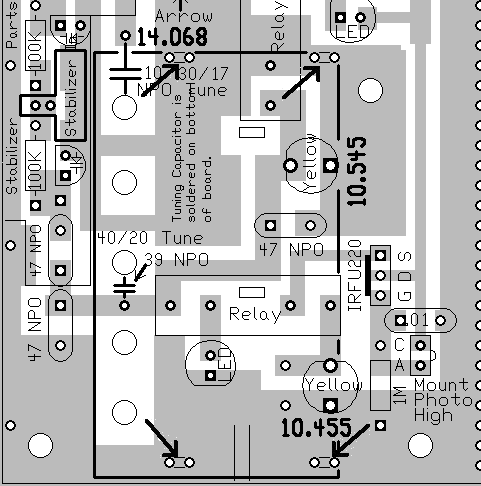
In the bottom middle of the board, Section 2, below the left edge of the left relay, below the 1K resistor, is a hole that is too close to the the 1K resistor and 12V Pad (notice the arrow). A spacer placed there will short to the pad. If you use a spacer/screw there you need to trim the pad a little so there is no short to the spacer or screw. |
|
The roll of tape is holding up the board so all the spacers can be seen. Using the spacers |
|
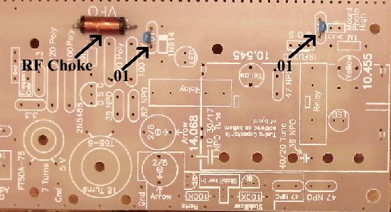
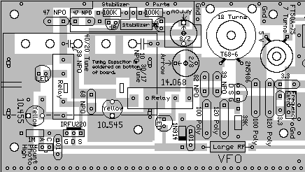
Begin each section by filling in the parts that have the value inside their footprint. They are the following: ____1 - Large RF Choke (Bag 3), Footprint on PCB is a rectangle with square edges, "Large RF" inside the rectangle. Choke is a wirewound choke about 1/2" long with black plastic ends. |
Resistors:
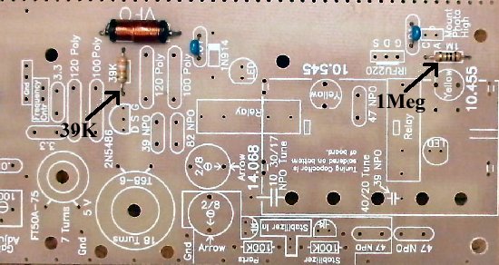
____1 - 1M (Bag 4), Next to photo diode in lower right hand corner. |
|
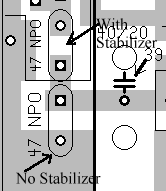
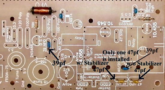
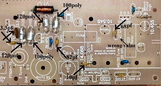
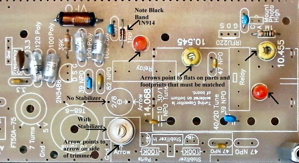
____1 - 47pf NPO (Bag 5), Orange colored, small square, labeled "470, JCC". Placement of this capacitor depends on whether you are using the stabilizer. If using the stabilizer, capacitor goes inside the stabilizer parts box as shown in the picture above. If not using the stabilizer, capacitor is put in the bottom footprint outside the box. |
|
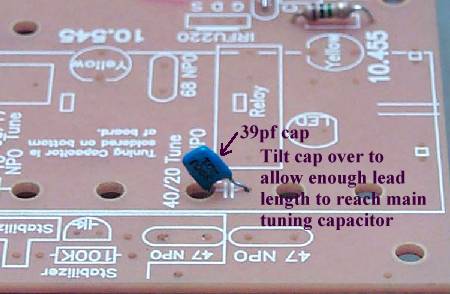
The second 39pf is located at the tuning capacitor, leave one end unsoldered until the tuning capacitor has been mounted. Bend the capacitor toward the large hole so that most of the lead length is underneath the board. The short lead will barely reach the main tuning capacitor if mounted flush with the board. Push unsoldered lead against the PCB to keep out of the way. Some kits will have one with longer leads. |
Solder
|
____2 - 3.3pf NPO (Bag 4), Orange colored, small square, leads flared out, labeled "3R3 D", or short leads, grey with black top, labeled "3R3" (R looks like a P). Both located next to the "Frequency Cntr" box. May be a ceramic 3.3pf in kit, note different ones in the picture. |
|
Note: Be careful not to splash solder on the Poly capacitors. Do not remove the solder if you get any on the poly caps. It will be very difficult to remove and could destroy the capacitor. Just check to make sure the solder is not touching one of the lead wires. Solder |
Other Parts:
____2 - Yellow Trim caps (Bag 1), Next to relays, note flat area on body and match to the flat on the footprint. |
|
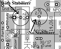
____1 - 2/8 Ceramic Trim cap (Bag 1), Note arrow over one leg, match the arrow on the trimmer to the arrow on the footprint. Clean and tin pins for a good connection when soldering on the board. Note: Placement depends on whether you are using the stabilizer. If you are using the stabilizer, the trimmer goes inside the stabilizer parts box as shown above and in picture below. If you are not using the stabilizer, the trimmer goes next to the 14.068 text. |
|
Be careful soldering the yellow trimmers, the tabs are difficult to solder. Check the following picture and make sure yours does not look like this: 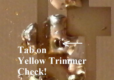 Add more solder to fix. |
|
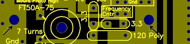
____1 - Photodiode (Bag 4), Square body with tiny bubble, mount with bubble as shown on footprint, Mount as high as possible straight up. Short lead is cathode "C". See inset in picture below (upper right side). Solder ____1 - IRFU220 (Bag 2), static sensitive part, please touch a ground wire before taking it out of the bag. Note thick white line on footprint, this shows where the heat sink of the part should be mounted. Marked "FU220, IR 625T, 32 03".____1 - 2N5486 (Bag 4), Spread the end pins slightly so they fit through the holes. Do not force all the way down onto the PCB and stress the pins. Note flat side of part and match to the flat side of the footprint. Solder |
|
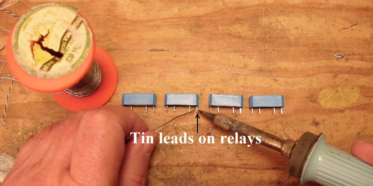
____2 - Blue Relays (Bag 4), Do not bend the pins of this relay when mounting/soldering on the PCB. The pins are very fragile. Orientation does not matter (Coil is the two center pins, relay is the two outer pins).
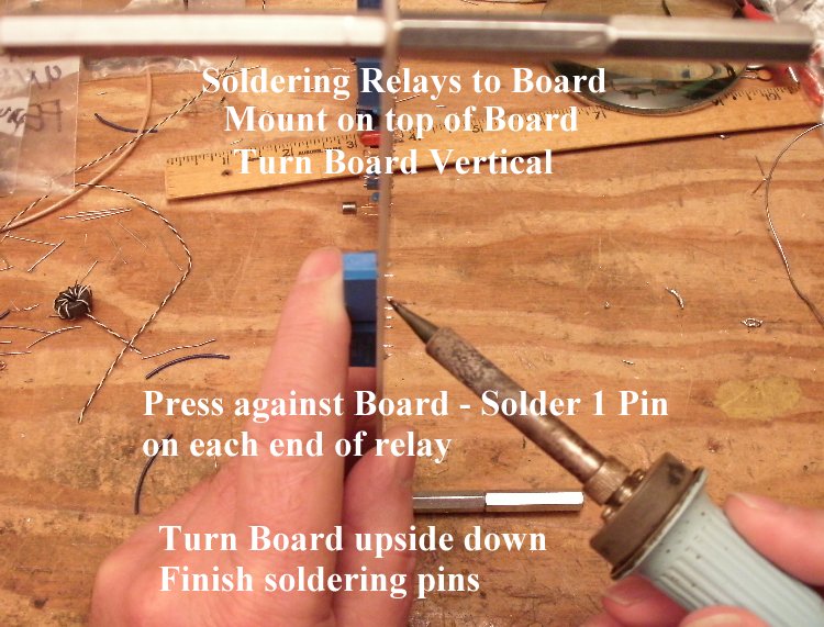
Solder each one individually Important Blue Relay mounting information! 1. Clean and tin the pins with solder before mounting to ensure a good solder joint. Wipe the excess solder to the top of the pin so the pins will fit in the holes. The pins can be difficult to solder without pre-tinning. |
|
2. Be sure to mount the relays flush with the board. If mounted slightly off the board, the relay will flex back and forth while handling the board, and break the pins between the relay and PCB. |
|
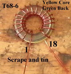
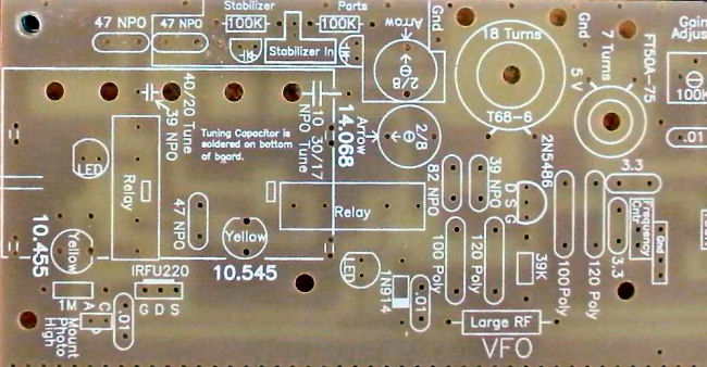
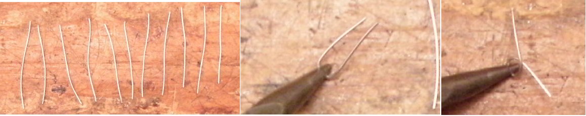
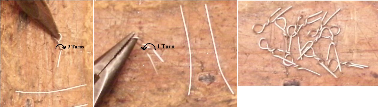
____1 - T68-6 toroid core, enameled wire (Bag 6), Pre-wound, as per instructions under the title "Preparation". Do not tie down on the board until the 14 MHz frequency has been set.
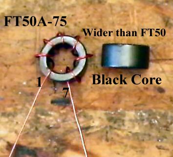
You can use a tie wrap, using the center hole and any hole around the core, or use a screw and nut with a 3/16" rubber grommet inside the toroid. (Parts not provided in kit) ____1 - FT50A-75 Ferrite Core, enameled wire (Bag 4), Pre-wound as per instructions under the title "Preparation".A small 3/16" grommet can be cut to fit inside the core, and with a 3/4" long screw and nut (4-40's), use the hole in the middle of the footprint to hold the ferrite core onto the board. (Parts not provided in kit) 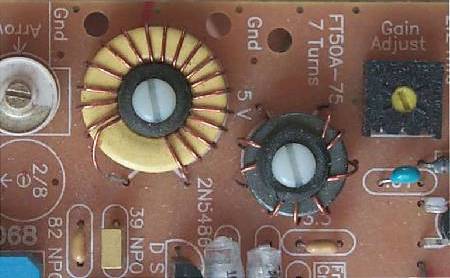 This picture shows the VFO and RF Choke held down with 4-40 nylon screws, 3/16" rubber grommet, and a metal 4-40 screw underneath the board. |
Solder
|
Arrows point to the dual holes and tiny rectangles that indicate where the feet of the main tuning capacitor will be soldered. Note the outline of the capacitor. The main tuning capacitor is soldered underneath the board. Small U shaped wires are placed in the holes and held down with masking tape. Then the board is turned over and the legs are soldered to the U shaped wires and the ground plane. ____1 - 5 section tuning capacitor (Bag 1), Because of its weight and size, best to mount after all the other parts have been mounted on the PCB. Information for mounting the tuning capacitor is at the end of the instructions for Board 1: First Mixer, Post-mixer Amplifier, Crystal Filters. |
This part of the PCB is not used if you are only going to use a DDS VFO..
No parts are installed in the VFO Section of the PCB
|
If you are using both the Vackar VFO and the DDS VFO, either now or later on, the VFO section above should be finished with the instructions above. |
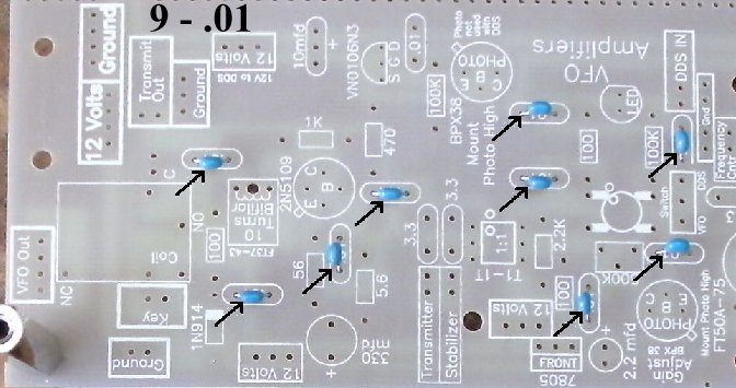
VFO Amplifiers____9 - .01 capacitors (Bag 3) |
|
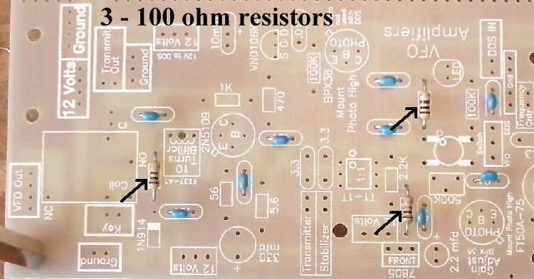
____3 - 100 ohm resistors (Bag 3), (brown, black, brown) |
|
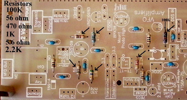
____1 - 100K resistors (Bag 3), (brown, black, yellow) |
|
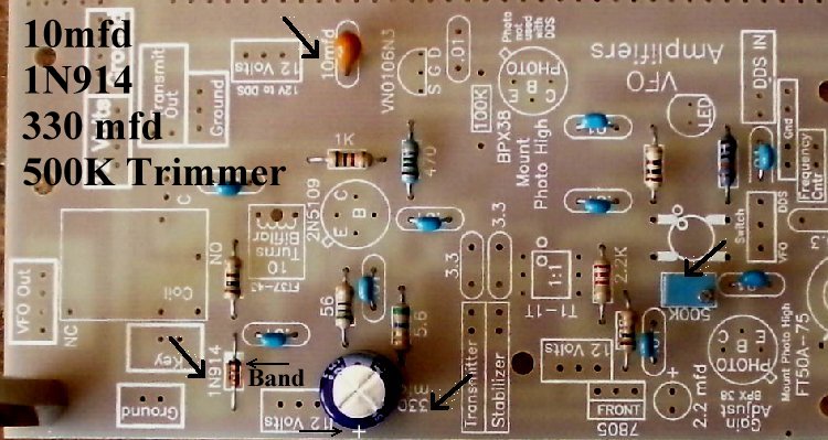
____1 - 10mfd Tantalum, 3 pin (Bag 4), The center pin is positive, two outer ones are ground, this part is used in automatic insertion PCB work so that it never gets put in wrong. Orange colored, with three short pins. |
|
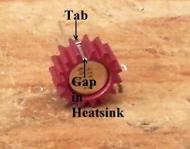
____1 - 2N5109 transistor and heatsink (Bag 6) |
|
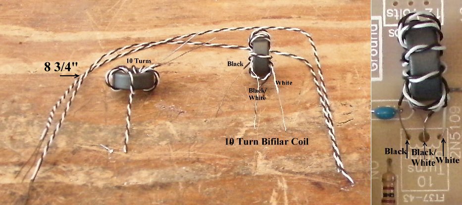
____1 - FT50-75 ferrite core (Bag 4) and wire (Bag 6) Note: Only one of the Black/White wires are used. |
|
____1 - T1-1T Minicircuits transformer (Bag 4), Note the dot on the T1-1T transformer and match the dot on the silkscreen. The dot on the outside of the footprint can be seen after the part is mounted so that you can double check proper mounting. ____1 - Wire jumper - a short wire cut from an installed resistor will work |
|
If you are using the Vackar VFO or both the Vackar VFO and a DDS VFO, place the SPDT slide switch in the Switch footprint. ____1 - SPDT Slide Switch |
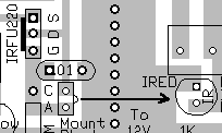
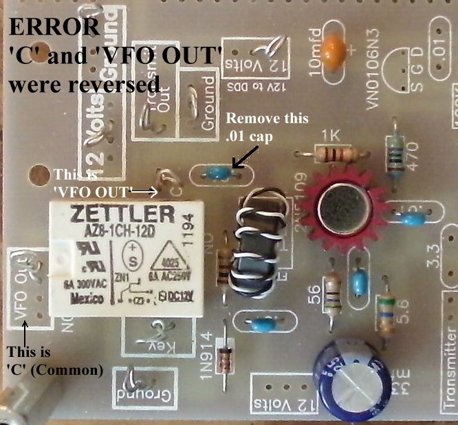
Relay Error FixA mistake was made on labeling the relay pins. The 'C' pin and the 'VFO OUT' pins are reversed. The 'C' pin is the common of the relay and the 'VFO OUT' is the Normally Closed pin. Use this text and the pictures to make this fix. The .01 cap that takes the output of the 2N5109 from the center connection of the Bifilar coil is removed between the connection to the Bifilar coil and the labeled 'C' pin on the board. |
|
The small coax cable will be connected after the board is populated. You can do the fix below now. Take a new .01 from the cardboard strip, but do not cut it off, keep the full length of the leads and clean them. Solder the .01 between pad that goes to the center of the Bifilar coil (there will be a hole there from the removal of the old .01 cap) to the pad near the edge of the board that is labeled 'VFO OUT' on the top of the board. You can run one wire of the cap through that open hole to help mount the new .01 cap. Remember to clip the excess wire of the .01 on the top side of the board when finished soldering. Solder the shield of the coax cable to the ground plane next to its new location right next to the other hole of the old .01 cap. (Labeled 'C' on top of the board) Next, solder the center conductor of the coax on that pad which has the hole for the old .01 cap. |

Checking Your Work |
|
____Check the dot on the MOSFET and the Minicircuits transformers. |
Send E-Mail || Amateur Radio Receivers || Back to Instructions for the SuperLuminescent Receiver